Question 705044
SCQMEDIUM
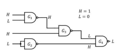
The logic levels and at different locations in a digital circuit are found to be as shown in the figure. Based on these observations, which of the logic gates is not behaving as an ideal NAND gate?
(A)
(B)
(C)
(D)
Detailed Solution
A NAND gate outputs only when both inputs are . Looking at , the inputs are and . The output is given as . An ideal NAND gate with inputs should yield (since , NOT ). Since the output is , is not behaving as an ideal NAND gate.
Free Exam
Boost Your Exam Preparation!
Move beyond just reading solutions. Access our comprehensive Test Series, original Mock Tests, and interactive learning modules. Many premium tests are completely free!
- Original Mocks & Regular Test Series
- Real NTA-like Interface with Analytics
- Many Free Tests Available